
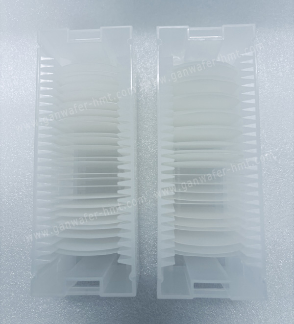
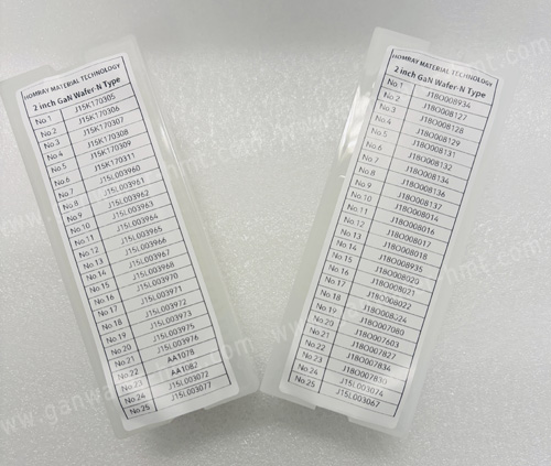
GaN on Sapphire Substrate Wafer Manufacturers
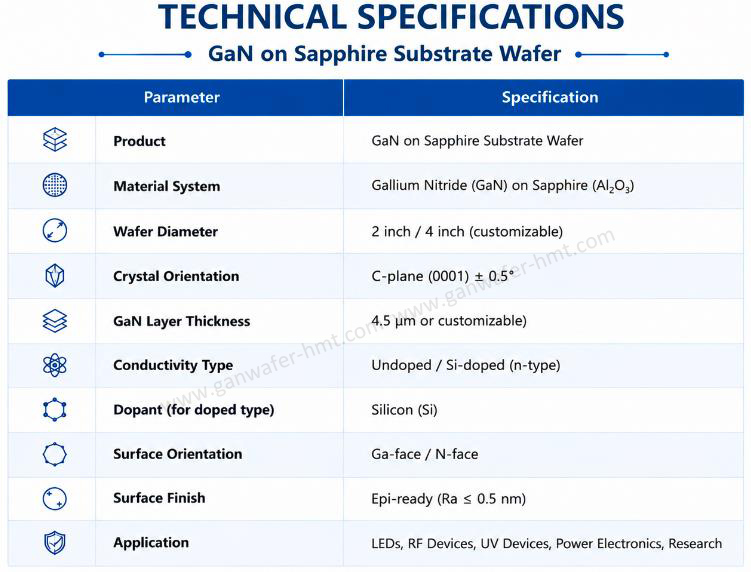
Dimensions: Ф 50.8 mm ± 0.5 mm
Thickness:4.5µm
Orientation:C-plane(0001) ± 0.5°
Useable Surface Area:> 90%
Product Description
GaN on Sapphire Substrate Wafer
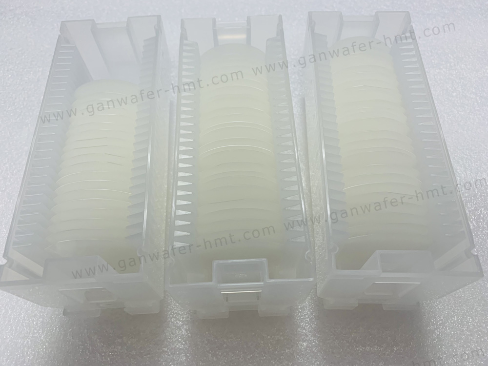
HMT provides high-quality 2inch 4inch and 6inch GaN on Sapphire Substrate Wafers for semiconductor manufacturers, research institutes and device developers worldwide.
A GaN on Sapphire substrate consists of a high-quality gallium nitride layer integrated with a sapphire supporting substrate, providing an excellent material platform for optoelectronic devices, RF components and advanced semiconductor applications.
Compared with traditional semiconductor materials, gallium nitride offers superior characteristics including wide bandgap, high breakdown electric field, high electron mobility and excellent thermal stability. By combining the outstanding properties of GaN with the cost advantages and mechanical reliability of sapphire substrates, GaN on Sapphire wafers provide a practical solution for large-scale semiconductor device development.
Key Features
High Quality GaN Crystal Structure
Our GaN on Sapphire substrate wafers feature:
- Excellent crystalline quality
- Low defect density
- Uniform GaN layer thickness
- Smooth surface morphology
- Stable wafer performance
Cost-Effective Semiconductor Platform
Sapphire is widely adopted as a GaN supporting substrate due to:
- Excellent mechanical strength
- High temperature stability
- Good chemical resistance
- Large-scale manufacturing capability
- Competitive cost advantage
Reliable Device Fabrication Platform
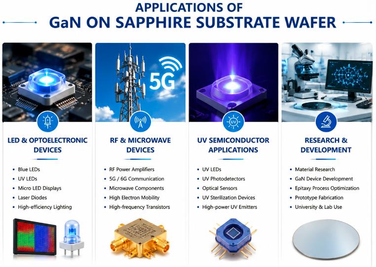
GaN on Sapphire substrates are suitable for:
- Optoelectronic device fabrication
- High-frequency semiconductor research
- UV device development
- Advanced GaN device structures
Why Choose HMT?
HMT specializes in advanced GaN and semiconductor substrate materials, supplying reliable wafer solutions for global customers.
Our advantages:
✓ Professional GaN material manufacturing experience
✓ Stable wafer quality and consistency
✓ Customized wafer specifications
✓ Support for research and production requirements
✓ Global semiconductor supply capability
HMT is committed to delivering high-performance GaN on Sapphire Substrate Wafer solutions for next-generation semiconductor technologies.Compared with free-standing GaN substrates, GaN on Sapphire Substrate Wafers provide a more cost-effective platform for optoelectronic and semiconductor device development.
Why use sapphire substrate for GaN devices?
Sapphire provides excellent mechanical stability, thermal resistance and cost advantages, making it one of the most commonly used supporting substrates for GaN devices.
What sizes of GaN on Sapphire wafers are available?
HMT provides 2 inch and 4 inch GaN on Sapphire substrate wafers with customized specifications according to customer requirements.
Related Products


 E-mail: kim@homray-material.com tina@homray-material.com
HMT Silicon Carbide (SiC) Substrate Website: www.sicsubstrate-hmt.com