
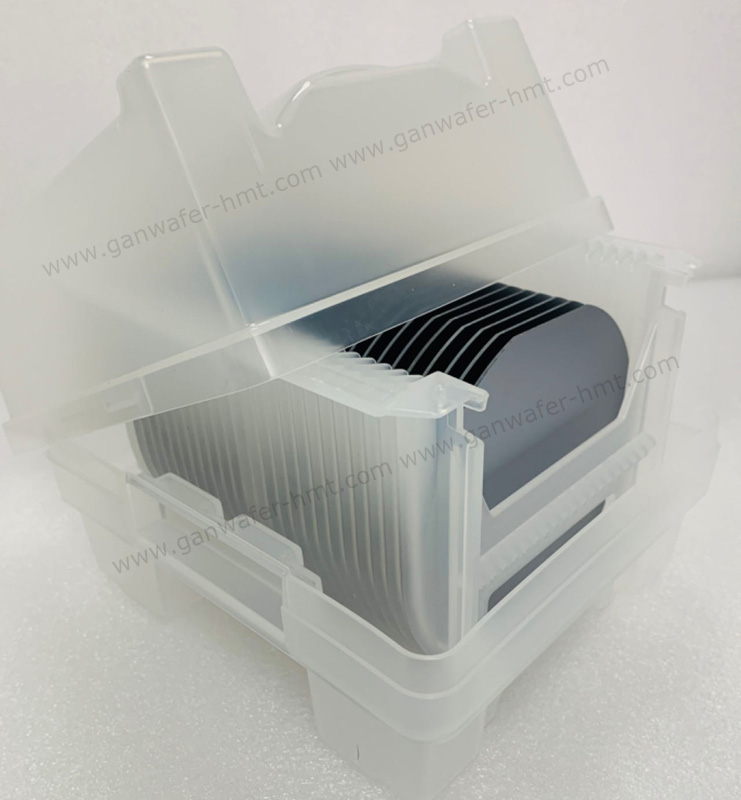
4 inch uid-GaN on Si Epi Wafer Manufacturers
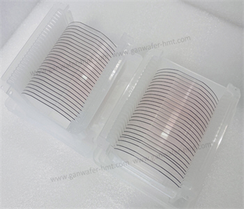
GaN-On-Si Epi Wafer
uid GaN Structure
Substrate Diameter: 2-8 inch Silicon
Substrate Thickness: 675,1000um
Product Description
Homray Material Technology provides high-performance unintentionally doped GaN (uid-GaN) on Silicon epitaxial wafers optimized specifically for advanced MEMS piezoelectric sensors and high-frequency SAW/BAW resonators. By utilizing high-purity MOCVD growth, our uid-GaN on Si epi wafers minimizing electrical leakage in piezoelectric transduction. This commercial-grade product delivers superior electromechanical coupling factors (k2>2.0%) and high thermal stability up to 600∘C, making it the industry standard for high-sensitivity strain, pressure, and acoustic wave sensing.
How does uid-GaN on Si enhance piezoelectric sensing performance?
Unintentionally doped GaN retains intrinsic polarization properties without free-carrier shielding, which drastically increases effective piezoelectric coupling coefficients under mechanical strain. Experimental data demonstrates that high-purity C-plane (0001) uid-GaN thin films achieve a Longitudinal Piezoelectric Coefficient (d33) of 3.1 pm/V, significantly outperforming conventional polycrystalline AlN thin films on silicon. Furthermore, the absence of intentional dopants reduces defect-assisted charge trapping, maintaining a high dielectric quality factor (Q>1500 at 10 kHz) across broad operating frequency ranges.
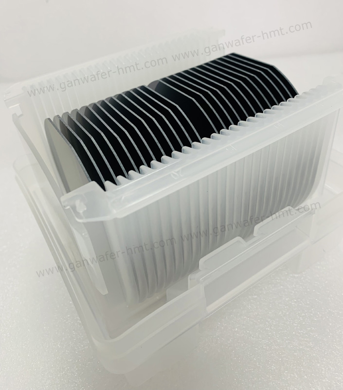
What are the key technical specifications of our uid-GaN on Si epi wafers?
Our MOCVD epitaxial platform ensures precise lattice transition engineering between the C-plane GaN layer and the Silicon (111) substrate through optimized AlN/AlGaN step-graded buffer layers.
| Parameter | Specification |
| Substrate | Silicon |
| Diameter | 2", 4", 6", 8" |
| Orientation |
<111> |
| Epi Layer Structure | uid-GaN/ AlGaN Buffer / Si Substrate |
| Surface Roughness |
<0.5 nm (5×5 µm2) |
How does this wafer facilitate cost-effective MEMS sensor manufacturing?
Growing high-purity uid-GaN on large-diameter Silicon substrates reduces fabrication costs by up to 65% compared to native GaN or sapphire-based alternatives. The total thickness variation (TTV) is strictly controlled to under 5 µm, enabling seamless integration with standard 6-inch and 8-inch CMOS/MEMS micro-machining process lines. To learn more about our broader product line, explore our [GaN Epitaxial Wafer Series] for high-power electronics and optoelectronic substrates.

Q1: Why is unintentionally doped GaN preferred over Si-doped GaN for piezoelectric sensors?
Unintentionally doped GaN (uid-GaN) keeps free carrier concentrations below 1×1016 cm−3, preventing free electrons from screening the internal strain-induced electric fields. This maximizes the piezoelectric output voltage and prevents high leakage currents in MEMS transducer devices.
Q2: Can these uid-GaN on Si wafers withstand high-temperature sensor processing?
Yes, our MOCVD-grown AlN/AlGaN strain-compensation buffer layers control wafer warp to under 20 µm. This structural integrity allows the wafer to withstand high-temperature MEMS processing up to 800∘C without crack generation or layer delamination.
Related Products





 E-mail: kim@homray-material.com tina@homray-material.com
HMT Silicon Carbide (SiC) Substrate Website: www.sicsubstrate-hmt.com