
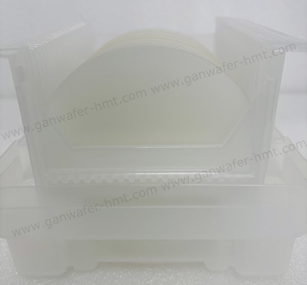
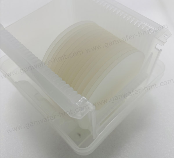
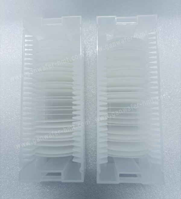
20 µm GaN Grown by HVPE on Sapphire
Dimensions: 2inch 4inch
Thickness: 20µm
Orientation:C-plane(0001) ± 0.5°
Useable Surface Area:> 90%
Product Description
HMT provides 20 µm GaN-on-sapphire wafers grown by Hydride Vapor Phase Epitaxy (HVPE) for semiconductor material research, thick GaN template development and subsequent epitaxial processes. A 20 µm GaN layer is significantly thicker than conventional few-micrometer GaN-on-sapphire templates, providing a different starting structure for projects that require a substantial GaN film. Research has demonstrated HVPE-grown GaN layers on sapphire at approximately 20 µm thickness, confirming this thickness range as a practical HVPE growth configuration.
The basic structure consists of a GaN layer grown on a C-plane sapphire substrate, with the GaN thickness specified at approximately 20 µm for this product configuration. The wafer can be considered when a customer needs a thicker GaN surface than the standard 4.5 µm GaN-on-sapphire template already available in HMT's product range.
Why 20 µm GaN-on-Sapphire?
A 20 µm GaN layer creates a substantially different template geometry compared with a 4.5 µm GaN layer. The approximately 4.4× thickness difference can be relevant when the GaN film itself needs to provide a thicker material platform for subsequent growth, structural processing or materials research.
The purpose of this product is therefore not simply to offer another GaN-on-sapphire wafer, but to provide a thick GaN-on-sapphire starting platform produced using HVPE. Published HVPE work has reported GaN layers ranging from 20 µm to 250 µm on sapphire-related template structures, demonstrating the scalability of HVPE for substantially thicker GaN growth.
HVPE as the Growth Route
Hydride Vapor Phase Epitaxy (HVPE) is a vapor-phase growth technique widely investigated for high-rate GaN deposition. In one published HVPE experiment, GaCl and NH₃ were used as the Ga and N precursors, with GaN growth performed at approximately 1050°C; the reported GaN thickness reached 20 µm.
Compared with conventional thin GaN epitaxy, HVPE is particularly associated with the growth of much thicker GaN layers. Published work has reported HVPE-grown GaN films from 250 µm to 300 µm on sapphire and free-standing GaN structures above 200 µm, illustrating why HVPE is an important technology for thick GaN material development.
Typical Wafer Configuration
| Parameter | 20 µm HVPE GaN-on-Sapphire |
|---|---|
| GaN Growth Method | HVPE |
| GaN Thickness | ~20 µm |
| Substrate | Sapphire |
| Orientation | C-plane (0001) |
| GaN Type | Un-doped / Si-doped |
| Wafer Diameter | 2 inch / 4 inch options |
| Surface | DSP/ SSP |
| Application | Thick GaN Template / Material Research / Epitaxy |
| Customization | Available according to project requirements |
HMT already supplies 2-inch and 4-inch GaN-on-sapphire templates, including a 4-inch configuration with a 100 mm ± 0.1 mm diameter specification, so these wafer formats provide a logical basis for the new product; the final 20 µm HVPE specification should nevertheless be confirmed before publication.

Applications of 20 µm HVPE GaN-on-Sapphire
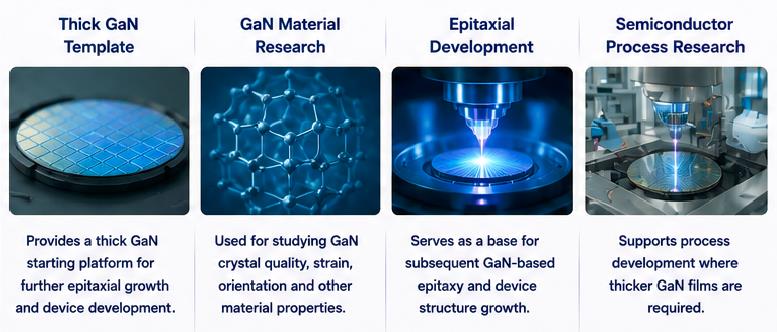
Thick GaN Template Development
The 20 µm GaN layer can provide a thicker starting platform for subsequent GaN material growth and structural development. Research has demonstrated HVPE-grown GaN templates with thicknesses substantially above 20 µm, showing the broader role of thick GaN layers in template development.
GaN Material Research
Researchers can use thick GaN-on-sapphire structures to investigate crystalline orientation, strain, surface morphology and other material properties. One published study specifically examined 20 µm HVPE-grown GaN using crystallographic and strain analysis.
Subsequent Epitaxial Growth
A thicker GaN platform can be used as a starting structure for additional GaN-based epitaxy or material-development studies. The appropriate surface condition and crystalline requirements should be defined according to the subsequent growth process.
Semiconductor Process Development
The 20 µm structure can also be evaluated for process-development projects in which the GaN film thickness is an important design parameter. The final suitability depends on the required surface morphology, stress, bow, defect density and downstream fabrication process.
Research and Prototype Development
A thick GaN-on-sapphire wafer can provide a practical experimental platform before moving to more expensive native or free-standing GaN substrates. Published HVPE studies have demonstrated both 20 µm-class layers and hundreds-of-micrometers-thick GaN films, providing a broad research basis for this material route.
20 µm HVPE GaN vs Conventional GaN Template
| Feature | Conventional GaN Template | 20 µm HVPE GaN-on-Sapphire |
| Typical GaN Thickness | 4.5 µm | ~20 µm |
| Thickness Ratio | 1× | ~4.4× |
| Growth Concept | Thin GaN template | HVPE thick-film growth |
| Substrate | Sapphire | Sapphire |
| Orientation | C-plane | C-plane (0001) |
| Main Role | Starting template | Thick GaN material platform |
FAQ
What is a 20 µm GaN-on-sapphire wafer by HVPE?
It is a sapphire-supported GaN wafer containing an approximately 20 µm GaN layer grown using HVPE. Published research has demonstrated 20 µm GaN growth on sapphire using HVPE.
Is 20 µm a standard or customized GaN thickness?
For this product, ~20 µm is the featured configuration. HMT can also discuss other GaN thicknesses according to the required wafer structure.For a conventional 2-inch GaN-on-sapphire template configuration, see our 2 Inch GaN-on-Sapphire Template. For applications requiring the sapphire substrate to be removed, see our Free-Standing GaN Substrate products.
Related Products


 E-mail: kim@homray-material.com tina@homray-material.com
HMT Silicon Carbide (SiC) Substrate Website: www.sicsubstrate-hmt.com